一、综述
参考:

7系列中,一个CLB包含两个slice:
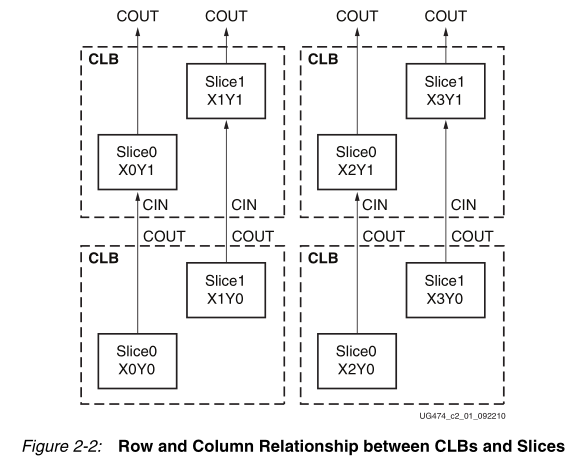
每个CLB的资源:

CLB可配置的主要功能:

二、主要功能
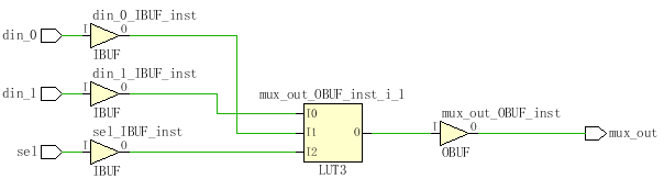
LUT是基本单元,例如选择器assign muxout = (sel) ? din_0: din_1;
A-shift register
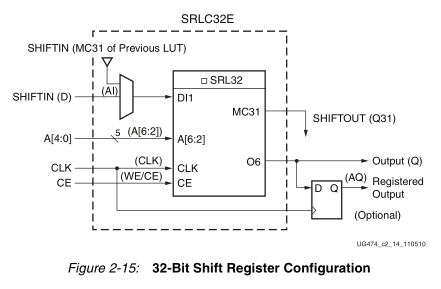
每个Slice对应4个LUT,而每个LUT可配32bit的移位寄存器:
对应指令:
always @(posedge clk) srl <= {srl[31:0],din};assign dout = srl[20]; 
当添加复位信号:
always@ (posedge clk) if(rst) srl <= 32'd0; else srl <= {srl[31:0],din]};assign dout = srl[20] 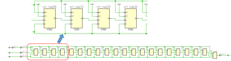
为什么结构不一致?因为LUT没有同步复位控制输入端,因此综合器无法将代码综合成有LUT实现的结构,因此写代码需要根据相应结构编写。
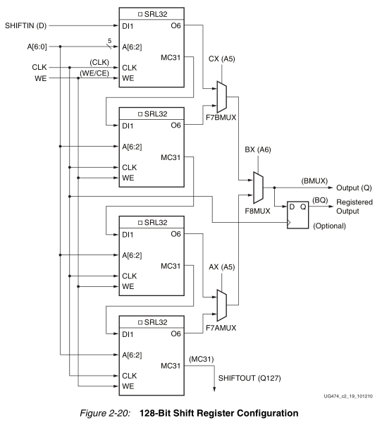
每个Slice可扩展为128bit的移位寄存器:
B-Distributed RAM
每个LUT为6选1,或2个5选1,其中SLICEM挂distributed RAM以及Shift Registers,关于Distributed RAM可实现的功能:
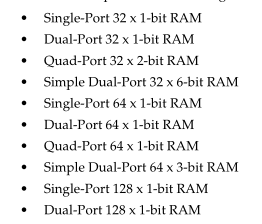
以下列举了一些适用于分布式RAM的情况:
1. 深度小于64-bit
2. 在深度大于64-bit小于128-bit情况下,有时延要求并需要异步输出(其clock-to-out时间小,并且布线比Block RAM自由) 3. 数据宽度小于16-bit(个人观点:这里配置RAM调用FPGA内部逻辑资源,而Block RAM blocks内部的RAM只能作为RAM使用,因此在时序没有要求,且固定RAM容量有剩余的情况下,不建议配置CLB中的RAM,固定RAM容量不够,可用CLB配置作为补充)。
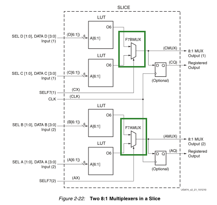
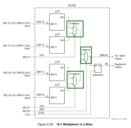
C-Multiplexer
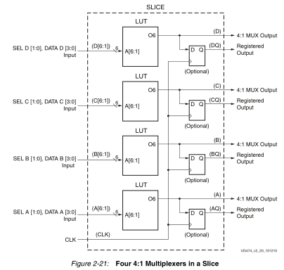
CLB还有一个重要功能:多路复用器(multiplexer)。
在一个Slice中包含有三个多路复用器:F7MUXA、F7MUXB和F8MUX。其中F7MUXA组合LUT A和LUT B成为7输入LUT,F7MUXB组合LUT C和LUT D成为7输入LUT,而F8MUX组合1个Slice中的4个LUT成为8输入LUT。

因此通过F7MUXA、F7MUXB和F8MUX的搭配,1个Slice可以实现4:1、8:1和16:1多路复用器,
- 一个LUT实现4:1多路复用器
- 2个LUT实现8:1多路复用器
- 4个LUT实现16:1多路复用器
如图1、2、3所示:
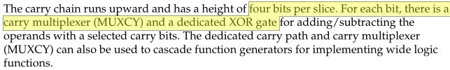
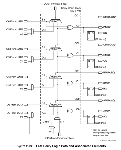
D-Carry logic
每个slice有4bits,每个bit包含一个多路复用和一个专用异或门XOR(用于加/减运算):
每个SLICE的Carry logic图:
三、原语
具体可参考,原语列表:
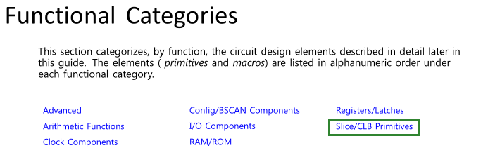
查看CLB相关的原语用法:
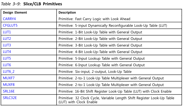
即可按需要进行调用,例如每个LUT对应32bit的shift register logic,查看原语:
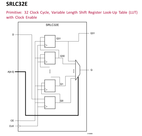
移位计算方法:

接口说明:

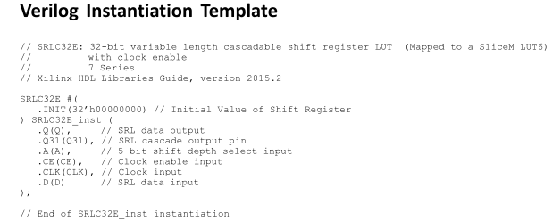
模板调用:
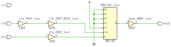
测试:
module CLB_SRL(clk,rst,din,dout);input clk,rst;input din;output dout;// SRLC32E: 32-bit variable length cascadable shift register LUT (Mapped to a SliceM LUT6)// with clock enable// 7 Series// Xilinx HDL Libraries Guide, version 2015.2SRLC32E #(.INIT(32'h00000000) // Initial Value of Shift Register) SRLC32E_inst (.Q(dout), // SRL data output.Q31(1'b0), // SRL cascade output pin.A(32'h00010100), // 5-bit shift depth select input.CE(1'b1), // Clock enable input.CLK(clk), // Clock input.D(din) // SRL data input);// End of SRLC32E_inst instantiationendmodule
综合之后的线路图: